
Title: Luminescent and Photoconductive Layered Lead Halide Perovskite Compounds Comprising Mixtures of Cesium and Guanidinium Cations
Authors: Olga Nazarenko, Martin Robert Kotyrba, Michael Wörle, Eduardo Cuervo-Reyes, Sergii Yakunin, and Maksym V. Kovalenko
Year: 2017
Journal: Inorganic Chemistry
Behind the technology used in digital electronics is fundamental research into semiconductors. Semiconductors are materials between conductors (metals) and insulators (rubber) in terms of conductivity. This semi-conducting behavior makes them easily manipulated for electronic application. The most simple type of semiconductor research is the discovery of new semiconducting materials. This research from Nazarenko et al. shows a new lead halide perovskite semiconductor. These structures are based on lead iodide/bromide, cesium, and organic ammonium groups. They investigate stability, optical properties, and photoconductivity, which is highly important for applications in thin-film electronics such as solar panels. Other lead halide perovskites are highly important right now for solar energy, as they are close in efficiency to commercial panels, but much less expensive to produce. Researchers are hopeful perovskites will make solar cheaper and more available. Exploring all related structures of lead halides, as this work does, is important to understand these materials and potentially make better solar panels.
Crystal Structure. Crystal structures are periodic ordered arrangements of atoms or molecules in 3D space. Think of a 3D grid, then place atoms at each corner or the center of each grid space and expand that same arrangement in all directions. This lattice (the grid) and atoms (basis) makes up a crystal structure. In this work, the chemists designed a crystal structure that inherently makes a 2D type network of atoms, with layers stacked on top of each other. There are inorganic layers of lead halide octahedra that make the 2D network, with layers of the organic ammonium and cesium separating the lead halide layers (Figure 1). This is a unique arrangement of atomic positions in perovskites, with alternating cesium and guanidinium (ammoniums) cations. This structure is analogous to the 2D perovskite structure or Ruddelson-Popper layered perovskite structure. These crystals were grown from a lead halide saturated solution in concentrated acid. The crystal structure was determined (solved) using a technique called x-ray diffraction, which uses the wave-nature of light to diffract off of the periodic atoms in the crystal structure. This diffraction pattern allows solving for the positions of the atoms. The crystal structures had formulas of: Cs(C(NH2)3]PbX4 (X = I, Br) and Cs2C(NH2)3Pb2Br7.
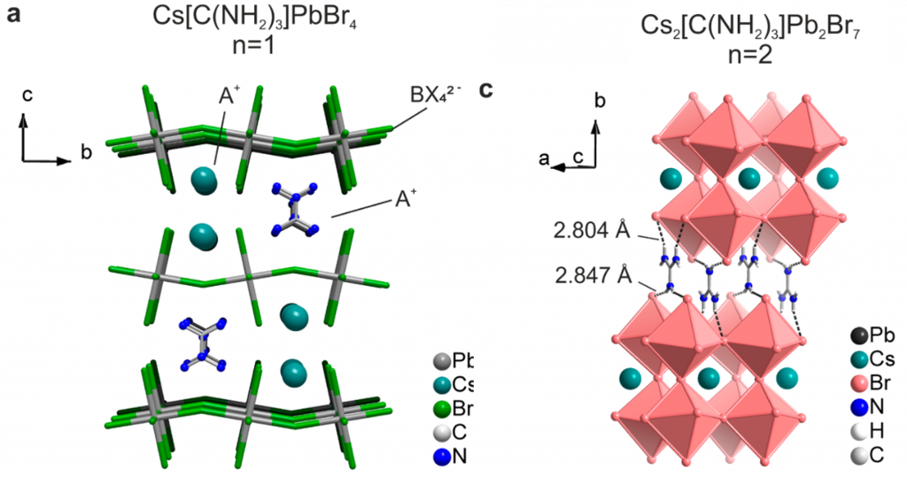
Figure 1. Crystal structure the compounds made in this work. These are the “Unit cells”, so take them, duplicate and translate them in every direction (a b c) to build the entire crystal.
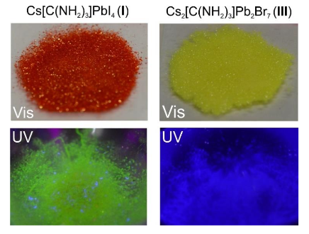
Characterizing a Crystal. Solving the crystal structures of new compounds is the first step of discovering new semi-conductors. Characterization by thermogravimetric analysis (TGA) was performed. This is heating the sample while measuring the change in weight of the compound. The compounds were heated to 300°C and above before large losses of weight began to occur, which shows this semi-conductor is stable for a variety of applications. This is important since very similar structures are not stable at these temperatures. Since these compounds are considered relevant for optoelectronics (optical or light based electronics), the light absorbance and emission data of the compounds were collected. The optical absorption data is a little different than a usual chemistry experiment. Absorbance spectra of solids cannot easily be collected in solution, the researchers put their crystals onto a glass slide held with transparent grease, and measured the amount of light that reflected off. This reflectance data is inversely proportional to the absorbance spectrum. The compounds show interesting absorption properties in that there is two absorption features per compound (Figure 2). First there is a large local maxima (bump) in the absorbance spectra, followed by a second, true maxima. The second large feature, is what typical semi-conductor absorbance experiments look like. They have broad areas of absorbance past a certain onset point (see band gap). The smaller feature, is due to absorbance from the quantum confinement affect. In these semi-conductors, the layered 2D planes of atoms are not like a “bulk” or 3D semiconductor, but act somewhere in between the behavior of a molecule and a bulk semiconductor. This is because the 2D perovskite structure is confined in one direction, (the direction the layer doesn’t grow). The lead halide semiconductors synthesized also have bright photoluminescence. Photoluminescence is the excitation of a compound with high-energy light, and the measurement of the photoemission produced (like white colors under a blacklight).
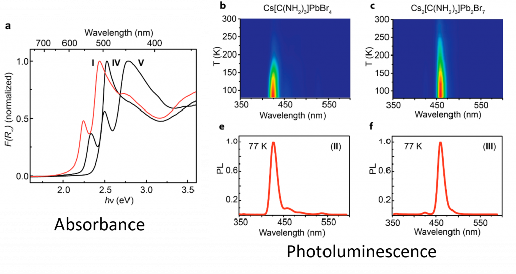
Figure 2. Absorbance spectra of the compounds. (Right) Photoluminecesnce of the compounds at varying temperatures, showing increased emission at low T
Basic Applications. A simple experiment these researchers did was to see how this new compound performs as a photodetector. A photodetector is simply a device that changes it’s electronic response based on how much light is hitting it, i.e. a constant voltage is applied, and current changes when illuminated. This compound had generous photoresponse, which gives it potential for applications and shows it behaves as expected. But this work is much more important than the photodetector. Showing new 2D layered perovskite structures made with cesium and organic ammoniums in arrangements like this, had not been demonstrated before. Knowing this crystal structure exists will be useful in characterizing other complex perovskites that are used in solar panels.