
Title: Gold Nanoparticle Plasmonic Superlattices as Surface-Enhanced Raman Spectroscopy Substrates
Authors: Cristiano Matricardi, Christoph Hanske, Juan Luis Garcia-Pomar, Judith Langer, Agustín Mihi, and Luis M. Liz-Marzán
Year: 2018
Journal: ACS Nano; DOI: 10.1021/acsnano.8b04073
Manipulation of light is essential for technologies such as solar panels, sensing, and communications. It’s so important, 2015 was designated by the United Nations as the International Year of Light and Light-based Technologies. At the heart of making these technologies work is fundamental research into materials that manipulate light in dramatic ways.
An essential part of light based technologies is the field of plasmonics. Plasmonics is the interaction of metals with light (electromagnetic radiation). When light is shined on a metal, electrons oscillate or resonate causing effects such as heating and the color of metals. In metals in the nanoscale size regime, electrons oscillate at specific frequencies (colors) of light controlled by the size and controlled periodic assembly of the nanomaterial. Because of this, nanoscale gold visibly changes colors with particle size. (Figure 1)

Figure 1. Size dependence of color in gold particles from smallest (left) to largest particles (right). nanocomposix
In addition to being able to change the color of light, nanoscale plasmonic materials absorb light more efficiently than their macroscale counterparts. This means the same amount of light is able to be utilized to a greater degree when it goes into a plasmonic material than a non-plasmonic material. This is highly desired in photovoltaics or imaging, both of which are dependent on how efficiently light is absorbed and utilized.
One of the major hindrances in the use of nanoscale plasmonic materials is the highly inefficient means of producing them. Useful periodic assemblies of plasmonic materials are currently made by complex lithography patterning processes which are expensive and time consuming. The most common way is producing patterns with electron beams, which is as expensive as it sounds. This is ok for high end, expensive applications, but to make these materials for the consumer markets, inexpensive techniques need to be discovered.
Here the researchers focus on a particularly important plasmonic material: gold nanoparticles and their assembly into arrays. Gold nanoparticles have high surface to volume ratio, and therefore exhibit surface-dependent manipulation of light. In addition their spacing in arrays affects how they absorb light. Both of these effects provide control over the color of the arrays.
These individual nano particles are simple to make and exhibit well understood plasmonic properties. However, when put into arrays, things like distance between particles or the way the ordered assembly occurs (called a superlattice), affects these plasmonic properties. But this is expensive to make and difficult to control.
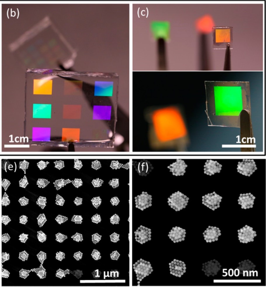
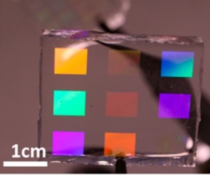
Figure 2. (Top) Pictures of the different colors which are dependent on the arrays. (Bottom) Scanning electron micrographs (SEM) of the arrays of clusters of nanoparticles made from the new stamping method.
These researchers have developed an extremely simple stamping method to make high quality arrays of gold nanoparticles. In this method, gold particles were dispersed onto a cheap, pre-patterned polymer (PDMS) and stamped onto glass in nanoscale arrays. (Figure 2). The method is extremely appealing for its simplicity relative to expensive lithography techniques. The particles assembled into supercrystal assemblies, which are periodic arrays of clusters of particles (Figure 2 Bottom)
To demonstrate how effective this simple method is, the size of the arrays was shown to be changed in a controlled fashion. The clusters of gold particles were made in the arrays with interparticle distances from 400 nm to 1600 nanometers (nm). (Figure 3).
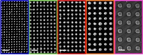
Figure 3. SEM images showing control of supercrystal assembly distance from 400 to 1600 nm (left to right)
There is a clear ability to control the color of the arrays. The larger the lattices were, the lower energy light was absorbed. A lattice array of 400 nm appears blue, which is a higher energy color than the red appearance of a 1600nm lattice array.
Utilizing nanoscale materials requires finding simple chemistry to control their production. Techniques such as this stamping method are simple, yet effective ways of making nanoscale materials that may be useful in the future. It’s easy to imagine stamping dyes composed of these particles in a precise manor on large-scale chips. A near-term application of this method is their use in nanoscale antennaes which would enable wireless commincations on an individual computer chip.
Figures reprinted (adapted) with permission from (Liz-Marzán, L. M., et al. ACS Nano 2018.). Copyright (2018) American Chemical Society.