
Title: Band Gap Tailoring and Structure-Composition Relationship within the Alloyed Semiconductor Cu2BaGe1-xSnxSe4
Authors: Garrett C. Wessler, Tong Zhu, Jon-Paul Sun, Alexis Harrell, William P. Huhn, Volker Blum, and David B. Mitzi
Year: 2018
Journal: Chemistry of Materials; DOI: 10.1021/acs.chemmater.8b03380
Advanced renewable energy sources are seen as essential for the energy profile of the future, those include better solar panels. Current commercial solar panels (aka photovoltaics) rely on expensive materials, which have the balance of efficiency and stability required for scaleable solar energy. Chemists and materials scientists are intensely exploring alternative materials to reduce the cost of solar energy.
One of the new materials with the potential to reduce is kesterite, Cu2ZnSn(S,Se)4 or CZTS. Kesterite is a crystalline material made of inexpensive, earth abundant, low toxicity elements; which makes it highly attractive for solar energy. However, kesterite has only reached solar power conversion efficiencies around 12% (Figure 1) compared to the best commercial silicon is at 22%. This relatively low efficiency is believed to arise from something called anti-site defects, which this research aims to fix.
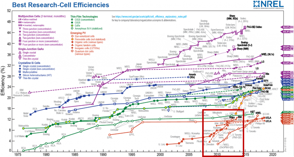
Figure 1. Research cell efficiencies, highlighting the recent rise in kesterite solar cells. (https://www.nrel.gov/pv/)
To understand anti-site defects, we first need to understand crystal structures. A crystal structure is a repeating arrangement of atoms. For a simple structure, like NaCl (table salt), every 5.6 Angstroms (5.6*10-10 meters) is a chloride ion in all directions along a cube (figure 2). In between each chloride sits a sodium ion. This repeats millions of times to make up entire crystal, such as those in table salt. All crystals have this periodic arrangement, but in the case of kesterite, it’s a more complex system of atoms.
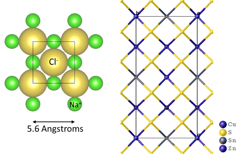
Figure 2. (Left) unit cell of a sodium chloride crystal structure showing the periodic arrangement of crystals. (Right) the complex crystal structure of kesterite showing the arrangements of tin/zinc/copper bridged by sulfur.
Kesterite is a crystalline mixture of tetrahedrons of Cu-S, Sn-S, and Zn-S, all bridged together by shared sulfide ions (Figure 2). Because Zn2+ and Cu2+ ions are close in size, it’s easy for the crystal structure to get mixed up. The Zn2+ cations can replace Cu2+ and vice versa. This is called an anti-site defect.
The result of these anti-site defects is a change in properties of the crystal. In other compounds, defects can be manifested in bulk properties, such as weakened mechanical strength. In kesterite, when Zn2+ and Cu2+ switch it creates atom scale electronic traps that stop the electrons from moving. Think of them like broken wires in a cable. This stops solar panels made up of kesterite from efficiently generating electricity.
One way to get around this defect site problem is to make better crystals. Crystal quality can be improved by using higher purity starting materials or slower, higher-temperature growth. These are the exact reasons silicon panels are so expensive, so it’s not as useful of a technique for improving the commercial viability of kesterite.
Another way to get around this defect site problem is to change the crystal structure itself. Here the problem is Zn and Cu switching easily based on size. What if element besides Cu or Zn is used?
The researchers probed this idea with theoretical calculations of potential crystal structures. They calculated how changing Cu or Zn with other elements would change the optical properties of the crystal structure. What they came up with was replacing the Zn2+ with a Ba2+ cation, which is much larger than Cu2+, and unlikely to have the anti-site defects.
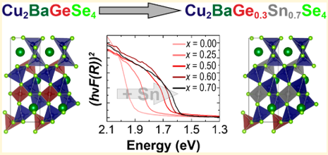
The researchers then synthesized and investigated the optical properties of powders of their new compound: Cu2Ba(Ge1-xSnx)Se4. By varying ratios of the germanium and tin, the compound could tailor the regions of light absorbed by the material (to better match sunlight). This was shown to be an effective compound in matching the solar spectrum.
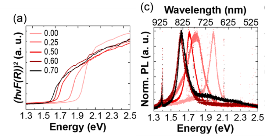
Figure 3. (Left) the absorbance spectra of kesterite with varying amounts of germanium added to the structure of Cu2BaGe1-xSnxS4, showing the tunable absorbance. (Right) the photoluminescence demonstrating the quality of the semiconductor.
A routine and reliable method to test the efficacy of a semiconductor is testing the photoluminescence. This is done by shining laser light on a semiconductor to excite it and observe the intensity and color of the emission (glow) of the semiconductor. The new kesterite based compounds showed fairly strong photoluminescence at room temperature, indicating this compound is a suitable semiconductor for PV applications.
This work highlights one method of improving a solar materials efficiency based on crystal engineering. This is a fundamental investigation into what can be done to change the properties of a material to make them more attractive in solar. It will be exciting to see how researchers expand upon this work, and most notably how efficient this new material is in a solar cell.
Images are “Reprinted (adapted) with permission from (Wessler, G. C.; Zhu, T.; Sun, J.-P.; Harrell, A.; Huhn, W. P.; Blum, V.; Mitzi, D. B., . Chemistry of Materials 2018, 30 (18), 6566-6574.). Copyright (2018) American Chemical Society.”