

Title- Nanodome Solar Cells with Efficient Light Management and Self Cleaning
Journal and DOI – Nano Lett. 2010, 10, 1979–1984, 10.1021/nl9034237
Climate change is real. It is not an opinion. It is not a coincidence. It is a fact.
So, I am not going to try and convince you that climate change is happening. Instead I am going to discuss a step further where each one of us should focus – the efforts towards sustainable development! The rapidly growing effects of climate change on the complex synergy of earth’s environment should be tackled at multifold level from individual contributions to policy change and big system operations.
A significant step towards sustainable development is generation of clean energy from renewable sources. Therefore, harnessing solar energy, the most abundant renewable energy source, has been the prime focus
of researchers for a very long time. Solar cells were first commercialized in 1956 in toys and radios but at a cost of 300$/Watt, which made it a luxury. Eventually in 1970s the cost was lowered to 20$/Watt and solar cells were extensively used to power satellites and oil rigs. Since then, several scientific advancements have brought down the cost of solar energy to 0.02 $/kWh-1 making it more affordable. However, to make solar energy our primary energy provider, there is still need for improvement in device performance and efficiency which will make its operational cost comparable to traditional energy sources.
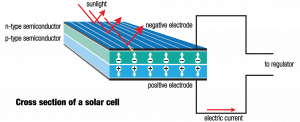
In this article, we will learn about one such development in solar devices which has improved their efficiency. Let us begin with understanding how solar energy is converted to electricity. The process of the conversion of sunlight (photo) into electricity (voltaic) is called the photovoltaic effect. These devices employ semiconductors like silicon which absorb the solar radiation and generate electric current. The absorption of solar energy depends primarily on the band gap of the semiconductor used in the device. Solar radiation with energy greater than or equal to the band gap will be absorbed and will excite electron into the conduction band where it is free to move and thus generating electricity. Figure 1 shows the working of a solar cell where the electron and hole are separated to generate current.
Silicon has been the most widely used photovoltaic material due to its suitable band gap of 1.1 eV which allows it to efficiently absorb most of the solar radiation. However, in addition to the material’s band gap, its geometry plays an important role in capturing the sunlight for absorption. A significant portion of sunlight incident on the device is lost due to reflection.
In the research article discussed here, the authors have developed a nanoscale architectural design to reduce the reflection of light and enabling upto 94% absorption of the incident radiation.
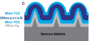
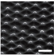
Figure 2 shows the nanoscale variation in their device. They have periodic dome shaped modulations in the device for all the layers along with the substrate which imparts the modulations from the cones present in it as shown in Figure 3. The semiconductor used is amorphous silicon which is sandwiched between layers of transparent conducting oxide (TCO) for conduction of electric current.
The authors compared their device performance with a flat solar cell made from the same material by characterizing the absorption of radiation of different wavelengths.
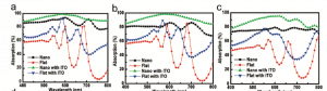
Figure 4 shows the absorption spectrum for flat vs nanodome samples with and without a conductive coating at different angles of incidence. It is important to perform the absorption measurements at different angles because the solar radiation in a practical environment is quite diffuse and will contact the device at multiple angles. In all the three cases, the black and green curve corresponding to nanodome samples have higher absorption for the entire wavelength range.
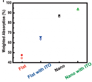
Figure 5 compares their absorption integrated absorption across the 400 – 800 nm range. The increased absorption percentage suggests that the periodic dome shaped modulations have anti-reflective effect, leading to light trapping and enhanced absorption.
In conclusion, novel nanodome devices have helped in improving device efficiency by trapping sunlight in their periodic modulations obtained from the substrate. In addition, this nanodome architecture design is not material specific and can be extended to other low-cost semiconductors which have been explored to substitute the expensive single crystalline silicon in solar cells. Also, its manufacturing is compatible with existing solar cell manufacturing technology, thus preventing any additional cost. These significant developments keep our hopes alive for making solar energy affordable, like traditional sources of electricity!